Advanced DFT course syllabus (16 weeks)
- DFT Basics
- SoC Scan architecture overview
- Types of Scan
- ATPG DRC Debug
- ATPG Simulation Mismatch Debug
- DFT Diagnosis
- JTAG
- MemoryBIST
- LogicBIST
- Scan and ATPG
- Test compression technigues
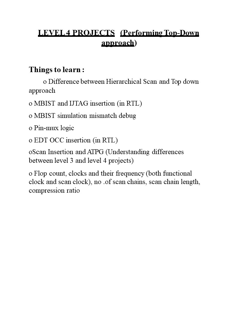
- Hierarchical Scan Design
- Introduction to DFT
- Roles in DFT
- Full SOC flow – DFT
- DFT Architecture and Basics
- Test Plan
- Different DFT schemes
- Comparison between Functional and DFT Vectors
- Defect, Fault and Error
- Revision of Digital Concepts
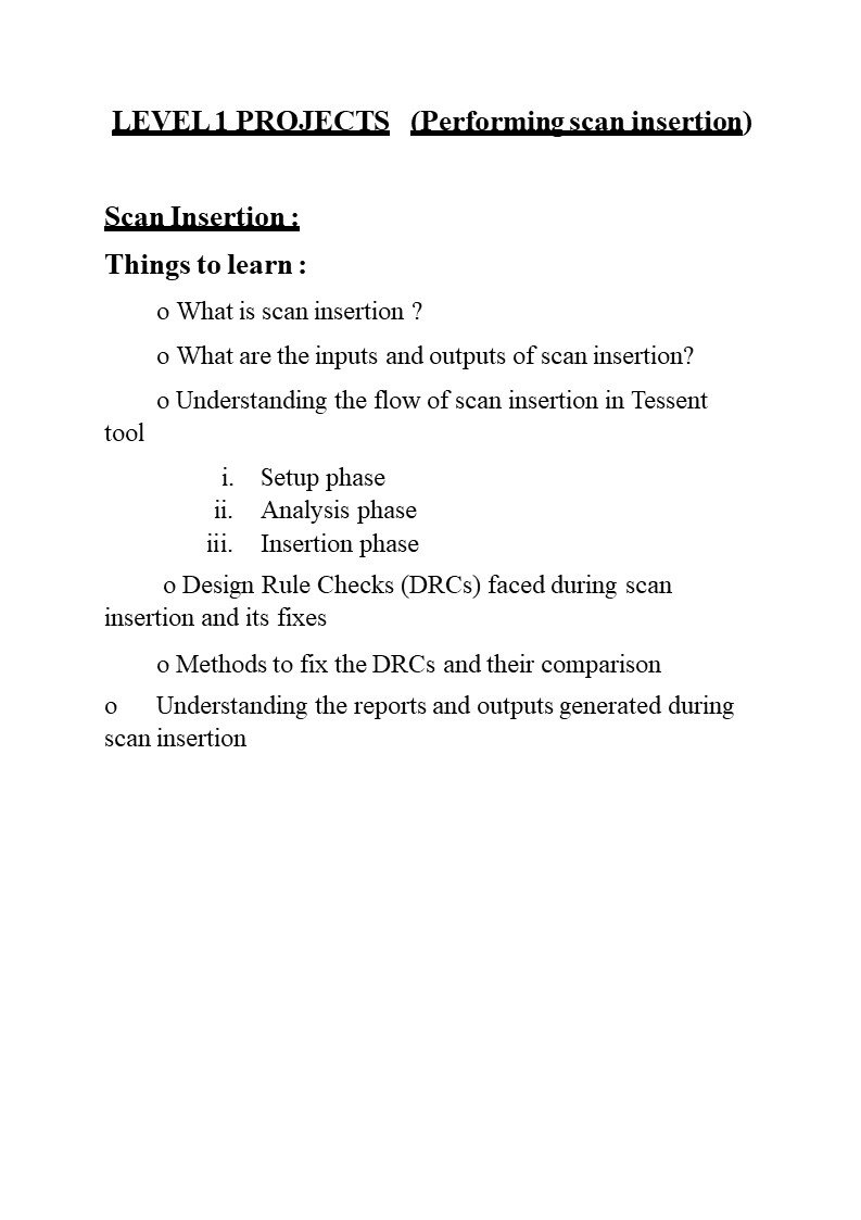
- Understanding of SCAN Insertion
- Scan methodology
- Types of Scan
- Top-down and Bottom-up Approach
- Scan insertion Flow
- Scan operation
- Clocking structure relation in SCAN
- DFT rule checks – Clock and Reset
- Scan insertion Scripts
- Multiple Clock domains
- DFT Rule Checks – Advanced (Tristate, PRC, XS)
- Precautions for building a proper scan chain
- Edge and Domain Mixing significance
- Scan Configurations
- Scan chain Balancing
- Lock up and Terminal lockup latches
- Hands-on Scan insertion
- Explanation about Netlist and Library files
- Assignments
- Hook-Up Scan sub chains
- Introduction to compression
- Compression Architecture
- Decompressor and Compactor
- LFSR
- Compression Ratio
- Masking Logic
- One hot Decoder
- Internal scan chains
- DRC Analysis
- Scan Reorder
- Control signals
- Modular Compression
- Introduction to Synthesis
- Hands-on Compression
- Assignments
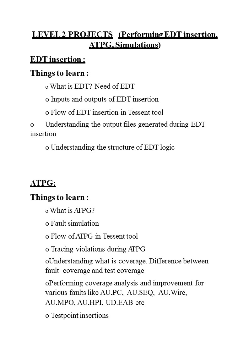
- ATPG Tools Introduction
- Fault Models
- Fault Categories
- Algorithms used in ATPG
- ATPG Flow
- Coverage Analysis
- Fault Classes
- ATPG DRC’s
- Hands-on Stuck-at ATPG
- Assignments
- Concepts related to STA – Basics
- MCP and FP
- Reports of ATPG
- Sequential Depth
- Transition delay faults (TDF)
- Path delay faults (PDF)
- Hands-on TDF ATPG
- Types of patterns
- Formats of patterns
- Fault grading
- LOC , LOS and LOES
- On chip clock control
- Advantages
- Dis-advantages
- Internal structure
- Introduction to Validation
- Simulations flow
- Tools for simulation
- Simulation mismatches debug
- No timing and Timing based Simulations
- Hands-on Simulations
- Flat Models
- Introduction to JTAG/IJTAG
- Introductions to PADS
- BS Insertion
- JTAG/IJTAG FSM
- Instructions of JTAG/IJTAG
- Introduction to MBIST
- Memory faults
- Memory grouping
- Memory basics
- Algorithms
- Zero-one, CHBK , MATS .MARCH ,SMARCH ..etc
- MBIST Insertion on RTL
- Hands on BIST insertion
- Assignments
- Discussion of Interview questions
- Compactor explanation
- Memory pipelining
- ET flow
- Hierarchical BIST insertion
- Hands of multi core MBIST insertion
- Assignments
- Complete Flow of BIST insertion and validation
- Clock Monitoring
- ICL network
- EDT and OCC insertion on RTL
- Gray box generation
- Assignments
- Introduction to ICL and PDL
- Scan Wrapper insertion – Hierarchical Flow
- Intest and Extest Hands on Lab sessions
- Assignments
- ATPG Flow with TSDB
- Faults merging
- Controlling PLL and CLK Gen’s using ICL and PDL
- Introduction to BISR
- Auxiliary Pins
- Revision of JTAG/IJTAG and BIST concepts
- Support for Mock interviews
- Interactive sessions
- Complete Revision of DFT as follows:
- DFT Overview
- SCAN
- COMPRESSION
- OCC
- JTAG/IJTAG
- MBIST/MBISR
- ATPG
- SIMULATIONS – ATPG and BIST
- Handling third party IP’s for DFT
- DFT Insertions in both RTL and NETLIST
- Total 4 levels of Projects in the entire course duration. Each Level contains 5-10 Working Labs.
Course Overview
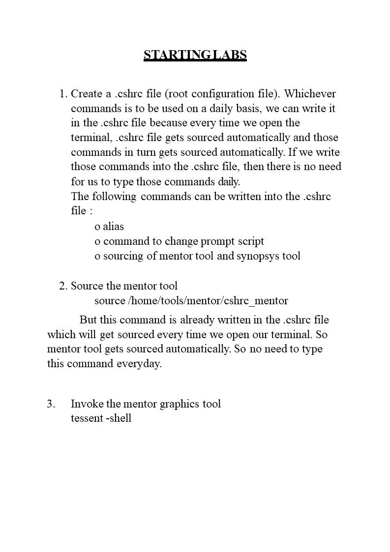
Mentor Graphics Tessent and Synopsys TetraMax (24*7 Tool access)
- Comprehensive training on full DFT flow including Scan, ATPG, BIST, and JTAG
- Hands-on experience with Tessent tool across all DFT modules
- Exposure to RTL and Gate-Level Netlist DFT implementation
- Focus on simulation, test compression, and debugging techniques
- DFT Basics and Fault Types (Stuck-at, Transition Delay, etc.)
- SoC Scan Architecture and Different Scan Types
- ATPG DRC and Simulation Debug
- DFT Diagnosis and Fault Analysis
- JTAG, MemoryBIST, LogicBIST Implementations
- Test Compression Techniques (TestKompress) and Hierarchical Scan Design
- Design featuring 17K+ flip-flops for real-world project simulation
- Lab exercises on each stage of DFT flow (Scan Insertion to Pattern Validation)
- Debugging and issue resolution from industry-level case studies
- Conceptual clarity paired with practical labs
- Delivered by experienced industry professionals
- Complete DFT training from RTL to Gate-Level flows
- Real-time projects and issue debugging using Mentor Tessent
- Focused on industry practices and tool proficiency
- Institute Info:
- Offered by VLSIGuru, established in 2012
- Trained over 10,000+ students
- Affordable in-class training in Bangalore
- Online training available for students outside Bangalore
Detailed overview:
Advanced DFT(Design for Testability) course is a 5 months course providing in-depth exposure to entire DFT flow including SCAN, compression, ATPG, simulations, JTAG and BIST techniques to add testability to the Hardware design. Participants will get hands on exposure to Tessent tool for all the aspects of DFT flow.
DFT Training focused on all aspects of testability flow including DFT basics, various fault types, SOC Scan Architecture, different scan types, ATPG DRC Debug, ATPG Simulation debug, and DFT diagnosis. DFT Training course will also focus on JTAG, MemoryBIST, LogicBIST, Scan and ATPG, test compression techniques and Hierarchical scan design.
Highlights:
- Design with 17K+ flip flops
- Exposure to all the aspects of flow both at RTL level and gate level netlist
- Multiple lab exercises on each aspects of the flow
- Exposure to issues faced in industry level project and how to resolve those issues


| Course | DFT Training |
|---|---|
| Duration | 16 weeks |
| Next Batch | 02/Aug |
| Schedule |
Saturday & Sunday 9AM – 1PM, theory sessions 2PM to 6PM, lab sessions |
| Course repeats | every 8 weeks |
| Tool | Synopsys Custom Compiler and Cadance Virtuoso {Mentor Graphics Tessent, Synopsys DFTAdvisor and Tetramax} |
| Mode of training | Both Classroom training and live online training |
| e-learning course for self paced learning | |
| Tool Access | Tool access for the complete course duration |
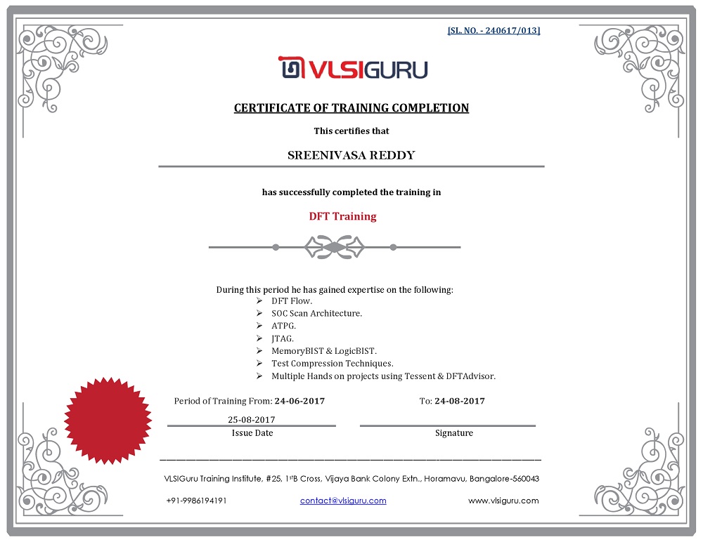
| Certificate | Course completion certificate issued |
| Batch Size | 20 |
| Assignments | 20 |
- Course presentations for all topics
- Session notes
- Lab documents with detailed steps
- User guides
- Course does not have any pre-requisites. However any exposure to Digital design, VLSI design flow is an added advantage.
- Each session of course is recorded, missed session videos will be shared
- Yes, You will have option to view the recorded videos of course for the sessions missed
- You will have option to repeat the course any time in next 1 year
- Yes, Course fee also includes support for doubt clarification sessions even after course completion
- You have option to mail you queries
- Option to meet in person to clarify doubts
Experienced Trainer
- Multiple trainers each with 15+ years of rich experience of working on complex SOC backend flow in various technology from 45nm to 7nm
- Multiple trainers with exposure to all the industry standard flow starting from Synopsys and Magma