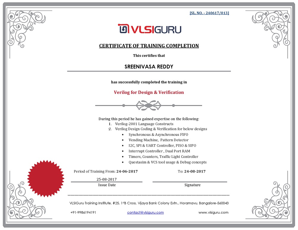
- Verilog language basics
- Verilog : How the language evolved?
- Verilog execution using Modelsim
- Verilog constructs
- Literals
- Data types
- registers, nets
- Vectors, Array
- Operators
- Various styles of Modeling: Data Flow, Behavioral, Gate level, Switch level
- Continuous assignments
- Combinational logic coding : Half adder, full adder, multiplexer, comparator, encoder, decoder, priority encoder
- Generate
- Procedural timing controls
- task and functions
- system task and function
- modeling memories and FSM
- Parameters
- Port connections
- Procedural blocks
- Sensitivity list
- State machines
- timescale
- Verilog timing regions
- process
- Blocking and nonblocking statements
- Inferring combinational and Sequential logic
- Clock generation with Duty cycle & Jitter
- Shift register implementation
- Procedural Blocks
- fork join
- Race conditions
- Synthesis examples
- Inter and Intra delay statements
- example to showcase race condition using blocking assignments
- Pipelining
- Memories
- Structural modeling
- Verilog Programming Interface(& PLI)
- PLI
- compiler directives
- system task usage: $display, $monitor, $strobe
- PLI, VPI implementation
- Primitive implementation using table, endtable
- DFF coding using gate level, behavioral
- Counters
- Up counter
- Ring counter
- Johnson counter
- Memory RTL coding and TB development
- Memory Verilog coding
- Declaring a parameterized memory
- Front door access
- Back door access test case coding
- Implemneting task for front door and back door access
- Test case coding and understanding waveforms
- FIFO – Synchronous FIFO and Asynchronous FIFO
- Synchronous FIFO
- Asynchronous FIFO
- Finite state machines
- Mealy and Moore style
- Implicit and Explicit styles of coding.
- Pattern detector – Overlapping, Non-Overlapping, Dynamic
- Overlapping
- Non-Overlapping
- Dynamic
- Traffic light controller
- APB protocol
- Interrupt controller
- SPI controller
- CRC generation
Course Overview
Verilog for Design & Verification is a 10 weeks course with detailed emphasis on Verilog for complex design implementation and verification. Verilog course helps both design and verification engineers to gain expertise in Verilog for RTL coding and test bench development.
Every aspect of Verilog course is supported with multiple examples to make the learning easier. Course also covers multiple design implementation examples and test bench setup for the same, and all these done from scratch.
Lab sessions are planned everyday to enable student work on these projects from scratch with trainer guidance.
Below is list of projects done as part of Verilog course. All these projects will be done in the live training sessions. All the codes will be done from scratch. There will be lab sessions where student will be doing the same with trainer guidance.
- Listing down design features
- Setting up Testbench and testbench development
- Testcase coding
- Debug the testcases and analyse the waveforms
- RTL Coding for both transmit and receive paths
- RTL integration
- Setting up Testbench and testbench component coding.
- Testplan development
- Testcase coding
- RTL coding and verification of Dynamic pattern detector
- RTL coding and verification of Watchdog timer
- RTL coding and verification of memory wrapper
- RTL coding and verification of Dual port RAM
| Course | Verilog for Design & Verification |
|---|---|
| Duration | 9 weeks |
| Next Batch | 25/May |
| Schedule | |
| Freshers | 6 days/week, 4 hours/day |
| Working professionals | Saturday & Sunday(9AM – 1PM IST) Access to all course recorded videos for entire course duration |
| Tool | Questasim & VCS |
| Mode of training | Classroom training & Live online training Course can also be done in hybrid mode. |
| eLearning with dedicated mentor for doubt clarifications. | |
| Fee | Live training : INR 14K + GST eLearning : INR 12K + GST |
| Batch Size | 25 |
| Assignments | 23 |
- Course presentations for all topics
- Session notes
- Lab documents with detailed steps
- User guides
- Each aspect of course is supported by lot of practical examples
- Dedicated full day lab sessions to ensure student does complete testbench development from scratch
- Yes, You will have option to view the recorded videos of course for the sessions missed
- You will have option to repeat the course any time in next 1 year
- Yes, Course fee also includes support for doubt clarification sessions even after course completion
- You have option to mail you queries
- Option to meet in person to clarify doubts
Experienced Trainer
- 10+ years of rich experience of working in Functional Verification domain across various mobile, networking, high speed peripheral domains.
- Experience of working on functional verification of Multiple Complex SOCs, multiple Sub systems
- Experience of working on multiple complex module level projects


- 1-1 Dedicated Mentor Support
- 24/7 Tool Access
- mock interview
- Industry Standard Projects
- Support with resume update
