Custom and analog layout 8 months course focused on all the aspects starting from Digital design, basics of semiconductors, fabrication, Linux, TCL scripting, Layout fundamentals, and detailed understanding of Analog, standard cell, memory and IO layout including physical verification.
Next Batch
1-1 Dedicated Mentor Support
24/7 Tool Access
Multiple Mock Interviews
Industry Standard Projects
Support with Resume Update
Custom and Analog Layout Training Overview
Custom Layout Training – Summary
Duration: 8-month comprehensive industry-oriented program
Tools:
- Synopsys Custom Compiler / Custom Designer
- Cadence Virtuoso
- 24×7 tool access provided throughout the program
Placement Support: VLSIGuru provides dedicated placement support until every candidate secures a job in the semiconductor industry.
Training Highlights:
- Analog Layout, Memory Layout, Standard Cell Layout, and IO Layout Design
- CMOS and FinFET technologies with real 18nm tech node exposure
- Various memory architectures and advanced layout techniques
- Detailed understanding of VLSI Design Flow and Advanced Digital Design
- Linux commands, scripting, version control, and soft skills for semiconductor interviews
Core Electronics Foundation:
- Semiconductors, Ohm's Law, and Kirchhoff's Laws
- Diode operation and MOSFET operation with second-order effects
- FinFET technology fundamentals and complete IC fabrication process
Layout Techniques:
- Standard Cell Layout Design — drive strength variants, multi-height cells
- Memory Layout and IO Layout for multiple architectures
- Analog Layout Techniques including Matching and Noise Mitigation strategies
- In-depth analysis of layout failure mechanisms: Electromigration, IR Drop, Antenna Effect, WPE, LOD, Stress Effects, Latch-up, and ESD
Hands-On Training:
- 20+ detailed lab sessions and structured assignments across all layout domains
- Real-time projects in Standard Cell, IO, Memory, and Analog Layout at 18nm tech node
- Hands-on practice using both Synopsys Custom Compiler and Cadence Virtuoso tools
Analog Layout Projects:
- Common Centroid and Interdigitation Techniques
- Resistor Matching and Capacitor Matching
- Opamp Layout, Current Mirrors, PLLs, ADCs, DACs
- Bandgap References and Temperature Sensors
- Current and Voltage Bias Lines, Large Drivers, LNAs, and Mixers
- Sense Amplifier and Bit Cell Development
Training Delivery:
- Comprehensive theory sessions paired with hands-on lab sessions
- Guided by industry expert trainers with real-time custom layout and analog design experience
- Practical exposure using real-time semiconductor design examples throughout the course
Program Highlights:
- End-to-end Custom Layout expertise — from CMOS and FinFET basics to advanced analog layout design
- Strong emphasis on layout failure mechanisms and robust, production-ready layout strategies
- Industry-standard EDA tool practices using Synopsys and Cadence Virtuoso integrated throughout
- Ideal for fresh graduates and engineering students targeting Custom Layout, Analog Layout, and VLSI physical design roles
- Suitable for engineers from non-layout domains planning to transition into custom IC layout and analog design careers
Institute Info:
- Offered by VLSIGuru, established in 2012
- Trained over 10,000+ students for semiconductor and VLSI careers
- Affordable in-class Custom Layout Training in Bangalore
- Online Custom Layout Training available for students and professionals outside Bangalore
- 24×7 EDA tool access on Synopsys Custom Compiler and Cadence Virtuoso
Detailed Overview
VLSIGuru's Custom Layout Training is an 8-month industry-oriented program that provides deep technical expertise across all major VLSI layout domains — including Analog Layout, Memory Layout, Standard Cell Layout, and IO Layout — using both Synopsys Custom Compiler and Cadence Virtuoso tools at a real 18nm technology node.
The course prepares fresh graduates and engineering students on all essential aspects of custom IC layout design — covering VLSI design flow, advanced digital design, CMOS layout, FinFET layout, memory architectures, standard cell design, IO design, and detailed analog layout techniques. Training also includes Linux commands, version control, scripting, and soft skills for effective semiconductor interview performance.
A strong electronics foundation is built through detailed sessions on semiconductors, Ohm's Law, Kirchhoff's Laws, diode operation, MOSFET operation, second-order effects, FinFET fundamentals, and the complete IC fabrication process — each followed by assignments and hands-on projects to reinforce understanding.
The course covers layout basics, hands-on standard cell layout, IO layout, and memory layout for multiple architectures, followed by comprehensive analog layout techniques — including in-depth discussions on mismatches and matching, noise and coupling effects, and critical layout failure mechanisms such as Electromigration, IR Drop, LOD and Stress Effects, WPE, Antenna Effects, Latch-up, and ESD — all commonly encountered in real semiconductor tape-outs.
Analog layout hands-on projects cover a wide range of industry-relevant circuits: Common Centroid and Interdigitation techniques, resistor and capacitor matching, Opamp layout, Current Mirrors, PLLs, ADCs, DACs, Bandgap References, Temperature Sensors, current and voltage bias lines, Large Drivers, LNAs, Mixers, and Sense Amplifier and Bit Cell development — giving students genuine production-level analog layout experience.
With 20+ detailed lab sessions, structured assignments, and multiple real-time projects, this Custom Layout Training program is one of the most comprehensive and hands-on VLSI layout courses available for freshers and engineers seeking to build careers in custom IC layout, analog layout design, and VLSI physical design at leading semiconductor companies.
VLSIGuru, established in 2012, has helped 10,000+ students build successful careers in the semiconductor and VLSI industry. The institute offers affordable Custom Layout Training in Bangalore and Online Custom Layout Training for students and professionals across India and beyond.
Synopsys custom designer and Cadence Virtuoso
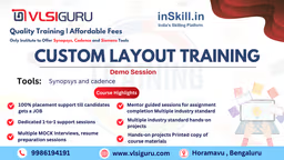

Key Features

Who All Can Attend This Custom and Analog Layout Training?
This training is ideal for individuals aiming to build or enhance their expertise in analog/mixed-signal IC layout design, especially for low-power, high-performance semiconductor applications. It is suitable for both entry-level engineers and professionals in the VLSI domain.Pre-requisites To Take Custom / Analog Layout
- Expertise on Digital & Analog design concepts
- Exposure to basic layout concepts

High Demand for Custom / Analog Layout
Know about the Growing VLSI industry
Analog Layout Engineers are in high demand in analog/mixed-signal and RF design teams. Engineers with experience in deep sub-micron nodes (e.g., 28nm, 7nm) and knowledge of DRC/LVS, EMIR checks, and parasitic-aware layout get premium salaries. Major hiring hubs include Bangalore, Hyderabad, and Noida.
₹6.5 LPA
₹10 LPA
₹14 LPA
₹18 LPA
₹22+ LPA

Bangalore remains the heart of India’s semiconductor ecosystem, offering strong opportunities in custom IC and analog layout design. For fresh graduates aiming to enter this niche domain, enrolling in a custom and analog layout training in Bangalore with real-time exposure is a critical step toward building a long-term career.
\n\n
A structured analog layout engineer training for freshers in Bangalore focuses on core layout concepts such as device matching, symmetry, parasitic extraction, and layout verification. For beginners, an analog IC layout course for freshers in Bangalore or a custom layout course for freshers in Bangalore helps build a solid foundation aligned with industry requirements.
\n\n
Learn with Real-Time Projects and Industry Workflows
\n\n
The key to mastering layout design lies in practical experience. Programs offering analog layout training with real projects in Bangalore enable learners to work on real chip-level designs and understand layout challenges in depth.
\n\n
An advanced VLSI analog layout training course in Bangalore incorporates Industry Standard Projects, structured assignments, and tool-based learning. With real time analog layout training with internship in Bangalore, candidates gain exposure to actual design flows used in semiconductor companies.
\n\n
Learners can opt for flexible online analog layout training course in Bangalore or choose an offline analog layout training institute in Bangalore depending on their learning preference.
\n\n
Internship Programs That Strengthen Job Readiness
\n\n
Hands-on experience is essential to transition into layout roles. A well-structured 6 months analog layout training and internship in Bangalore or a custom layout internship program with placement in Bangalore allows candidates to gain real-time exposure.
\n\n
Programs offering an analog layout internship with placement support in Bangalore or a custom layout internship for freshers in Bangalore help build practical confidence. A comprehensive layout design course with internship and placement in Bangalore ensures that learners are industry-ready by the time they complete the program.
\n\n
These opportunities are ideal for those seeking a job oriented analog layout course in Bangalore with a strong focus on real-world application.
\n\n
Designed for ECE, EEE, and Engineering Graduates
\n\n
A focused analog layout training for ECE students in Bangalore and analog layout training for EEE students in Bangalore ensures that candidates from electronics backgrounds can seamlessly transition into backend roles.
\n\n
Programs designed as analog layout training for fresh graduates with placement in Bangalore and backend analog layout training in Bangalore cover the complete full-custom design flow. A structured custom layout engineer training program in Bangalore prepares candidates to handle real-time design challenges confidently.
\n\n
Placement-Focused Training for Career Growth
\n\n
A placement oriented analog layout course in Bangalore plays a crucial role in helping candidates secure jobs in semiconductor companies. Programs offering analog layout training with placement in Bangalore include resume building, technical interview preparation, and Mock Interviews.
\n\n
A custom IC layout course with placement assistance in Bangalore or a custom layout course with job assistance in Bangalore ensures that candidates are fully prepared for hiring processes. Enrolling in an analog layout course with job assurance in Bangalore or custom layout training with placement in Bangalore aligns your skills with current industry expectations.
\n\n
For faster career entry, fast track analog layout training in Bangalore provides accelerated learning while maintaining strong practical exposure.
\n\n
Learn with Expert Guidance and Continuous Support
\n\n
A high-quality custom layout training in Bangalore program is supported by experienced mentors who bring real-world insights into training. With Expert Faculty Support, learners receive continuous guidance throughout their journey.
\n\n
Flexible options like a weekend analog layout training course in Bangalore make it easier for students and working professionals to upskill. Regular doubt clarification sessions, combined with structured learning, ensure consistent progress and confidence building.
\n\n
Start Your Career in Custom Analog Layout
\n\n
With increasing demand for layout engineers, enrolling in a full custom layout training in Bangalore is a strategic move for freshers. If you are searching for the best analog layout training institute in Bangalore, choosing the right program is essential.
\n\n
A comprehensive job oriented analog layout training in Bangalore or analog layout training for freshers in Bangalore equips you with both technical expertise and practical experience. With the right combination of training, internship, and placement support, you can confidently step into roles in custom IC and analog layout design within the semiconductor industry.

Explore a wide range of VLSI and Embedded Systems courses to get industry-ready.
50+ industry oriented courses offered.

Explore a wide range of VLSI and Embedded Systems courses to get industry-ready.
50+ industry oriented courses offered.