
Mr. Sreenivasa Reddy
Director
DIRECTOR'S MESSAGE
Teachers play a crucial role in a person's education. They have the power to make a subject either interesting or boring. At VLSIGuru, we make sure that all the sessions are engaging by correlating with real life examples and giving practical exposure to everything being taught.
We strive to ensure VLSIGuru is a place that makes a significant difference to your learning and career.
No courses available in Freshers
No courses available in Freshers

VLSIGuru Assurance
Train with courses designed and delivered by highly experienced industry veterans.


Training in latest technologies, with a co-created and co-curated curriculum.
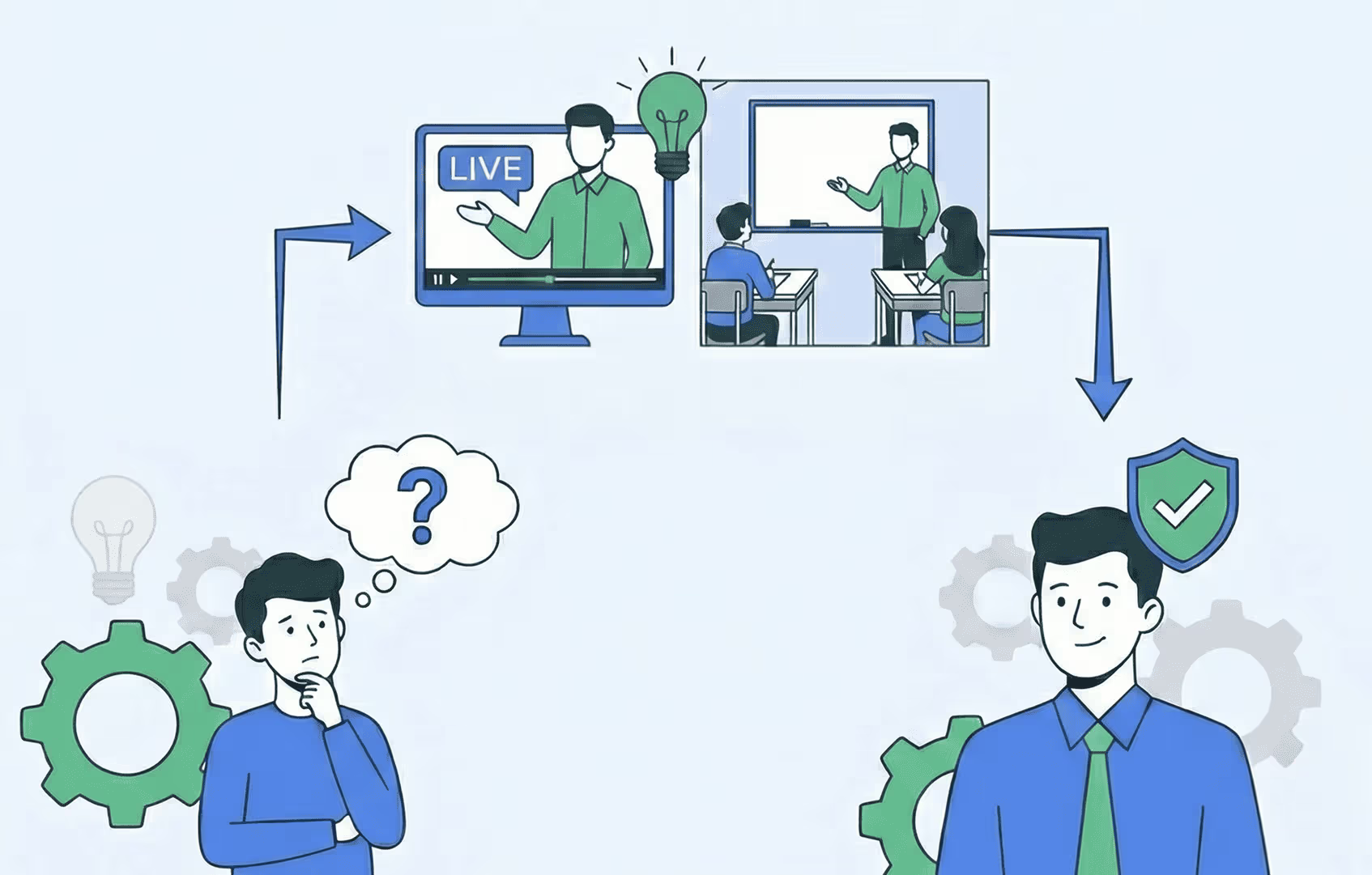
Get your queries resolved instantly with our live doubt clarification sessions. Trainers and mentors help you understand concepts from the basics, ensuring you gain complete clarity and confidence in every topic.

At VLSIGuru, we believe that education should lead to meaningful employment. Our training programs are designed not just to impart technical excellence, but also to bridge the gap between academic learning and industry demands. With a strong network of hiring partners and a proven track record, we ensure that our students are career-ready.
Placement Highlights
- Industry-aligned curriculum
- Hands-on projects and case studies
- Communication skills
- Resume building and interview preparation
- Technical and HR mock sessions
- Aptitude and domain-specific test series
- Regular drives and exclusive hiring events with partner companies
- Resume building and interview preparation

At VLSIGURU, we provide industry-focused VLSI training and guidance that helps students and professionals build strong technical skills and succeed in their careers. Our programs are designed to be practical, flexible, and aligned with current industry requirements.
Why TO Choose VLSIGuru?
100% job oriented VLSI training courses
BEST ADVANTAGES OF VLSIGURU
Explore advanced VLSI topics designed to meet the evolving demands of the semiconductor industry.
Get hands-on experience with industry-grade projects.
Learn from professionals with years of VLSI experience.
100% job-oriented training with placement guidance.
Inskill E-learning Platform
Self-paced learning courses in VLSI and Embedded systems with tool access and practical exposure to industry standard projects.
Frequently Asked Questions
Student Reviews


VLSI Functional Verification Training
- Ethernet MAC verification, DMA controller verification
- AXI VIP Development, AHB UVC development
- Hands on exposure to Questasim and VCS tools with 24×7 access
Physical Design Training
- Projects done at 14nm technology
- Projects on entire PD flow including Synthesis, STA, Redhawk and Physical verification
- Hands on exposure to Synopsys tools with 24×7 access
DFT Training
- Multiple projects covering all the aspects of the DFT flow
- Scan, ATPG, Compression, Simulation, JTAG, boundary scan, MBIST, LBIST and iJTAG
- Hands on exposure to Mentor graphics and Synopsys tools with 24×7 access
Custom Layout Training
- Standard cell layout, Memory layout, IO layout and Analog layout
- Includes circuit design, schematic, layout and physical verification
- Hands on exposure to Synopsys and Cadence tools
RTL Integration Training
- Focus on RTL design, Lint, CDC, UPF, Synthesis, STA, LEC and Core tools
- Projects covering all the aspects of integration flow
- Hands on exposure to Synopsys Spyglass, Formality, Design Compiler, PrimeTime, VCLP and Core tools
FPGA System Design Training
- Focus on RTL design and FPGA system validation
- Projects on FPGA system design flow
- Hands on exposure to Zed board
Embedded Systems Training
- Training on C, Data Structures, C++
- Micro-controllers, Embedded C, peripheral protocols, Linux drivers, RTOS
- Projects based on all these aspects
VLSIGuru Institute was set up in 2012 with the motto of ‘quality education at affordable fee’.
We have trained over 1500+ students and are among the very few institutes offering full-spectrum VLSI training including RTL design, Functional Verification, GLS, Synthesis, STA, Physical Design, DFT, Custom Layout and more.
Also offering advanced courses on AMBA, PCIe, USB, DDR, Low power verification, SoC verification tailored for experienced engineers.
© 2025 - VLSI Guru. All rights reserved
Explore a wide range of VLSI and Embedded Systems courses to get industry-ready.
50+ industry oriented courses offered.

Explore a wide range of VLSI and Embedded Systems courses to get industry-ready.
50+ industry oriented courses offered.


